Tesla has launched a targeted recruitment drive in Taiwan, seeking skilled semiconductor engineers for its upcoming “Terafab” initiative—an ambitious move aimed at strengthening its position in the rapidly evolving artificial intelligence (AI) chip landscape.
Recent job postings reveal that the company is hiring for multiple engineering roles, each requiring at least five years of experience in advanced semiconductor manufacturing.
The effort highlights Taiwan’s growing importance as a global hub for chip expertise, largely driven by industry leader Taiwan Semiconductor Manufacturing Company.
Inside the Terafab Vision
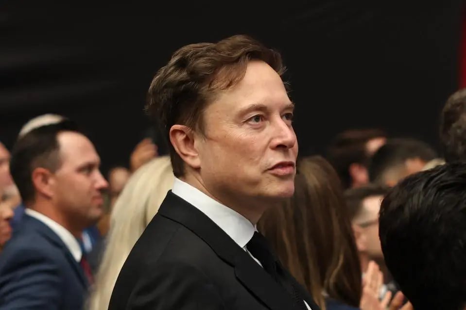
The Terafab project, introduced by Elon Musk, is designed as a fully integrated semiconductor manufacturing facility.
Unlike traditional fabs, Terafab aims to unify several critical stages of chip production—including fabrication, packaging, testing, and mask production—within a single ecosystem.
This vertically integrated approach is expected to improve efficiency, reduce reliance on external suppliers, and give Tesla tighter control over its semiconductor supply chain.
Focus on Next-Generation Chip Technology
Tesla’s hiring criteria indicate a strong emphasis on cutting-edge semiconductor processes.
Candidates are expected to have experience working with nodes below 7 nanometres, as well as familiarity with emerging 2-nanometre technologies—areas where Taiwan’s semiconductor ecosystem remains highly competitive.
The company is also prioritizing expertise in advanced packaging solutions such as CoWoS and SoIC, both pioneered by TSMC.
These technologies are crucial for high-performance computing and AI workloads, allowing for faster data transfer and improved chip efficiency.
Broad Engineering Scope Signals Scale of Project
The available roles span a wide range of technical disciplines, including lithography, etching, thin-film deposition, and chemical mechanical planarisation.
Tesla is also seeking specialists in yield optimization and process integration, underscoring the complexity and scale of the Terafab initiative.
Industry observers say this breadth of hiring reflects Tesla’s intent to build not just chips, but a comprehensive semiconductor manufacturing capability.
AI Demand Drives Strategic Shift
Tesla’s move comes at a time of surging global demand for AI chips, driven by advancements in machine learning, autonomous systems, and data-intensive applications.
The proposed Terafab facility is expected to support diverse use cases, from edge AI processors to satellite-grade chips and high-bandwidth memory systems.
While Tesla has yet to officially comment on the recruitment effort, the strategy aligns with a broader industry trend toward in-house chip development as companies seek to secure supply and boost performance.
Industry Experts Warn of Long Timelines
Despite the ambitious vision, experts caution that semiconductor manufacturing remains a complex and time-intensive process.
Taiwan Semiconductor Manufacturing Company has noted that building a new fabrication plant typically takes between two to three years, emphasizing that rapid scaling in this sector is rarely straightforward.

Outlook
Tesla’s expansion into semiconductor manufacturing through Terafab signals a deeper commitment to owning critical AI infrastructure.
If successful, the initiative could position the company as a more formidable player not just in electric vehicles, but in the global race for advanced computing power.